Board Description
More detailed description of LimeSDR XTRX board components and interconnections is given in the following sections of this chapter.
LMS7002M RF transceiver digital connectivity
The interface and control signals are described below:
Digital Interface Signals: LMS7002 is using data bus LMS_DIQ1_D[11:0] and LMS_DIQ2_D[11:0], LMS_EN_IQSEL1 and LMS_EN_IQSEL2, LMS_FCLK1 and LMS_FCLK2, LMS_MCLK1 and LMS_MCLK2 signals to transfer data to/from the XILINX FPGA. Indices 1 and 2 indicate transceiver digital data PORT-1 or PORT-2. Any of these ports can be used to transmit or receive digital IQ data. By default PORT-1 is selected as transmitter port and PORT-2 is selected as receiver port. The FCLK# is input clock and MCLK# is output clock for the LMS7002M transceiver. TXNRX signals are used to indicate ports direction. Please refer to LMS7002M transceiver datasheet page 12-13. [link] for the LMS7002M interface timing.
LMS Control Signals: these signals are used for the following functions within the LMS7002 RFIC: * LMS_RXEN, LMS_TXEN – receiver and transmitter enable/disable signals connected to FPGA Bank 14 (3.3V). * LMS_RESET – LMS7002M reset is connected to FPGA Bank 14 (3.3V).
SPI Interface: LMS7002M transceiver is configured via 4-wire SPI interface: FPGA_SPI_SCLK, FPGA_SPI_MOSI, FPGA_SPI_MISO, FPGA_SPI_LMS_SS. The SPI interface is connected to FPGA Bank 14 (3.3V).
LMS I2C Interface: can be used for LMS EEPROM content modification or debug purposes. The signals LMS_I2C_SCL and LMS_I2C_DATA are connected to EEPROM.
Chip pin (IC1) |
Chip reference (IC1) |
Schematic signal name |
FPGA pin |
FPGA I/O standard |
FPGA I/O standard |
|---|---|---|---|---|---|
E5 |
xoscin_tx |
LMS_TX_CLK |
Connected to 26.00 MHz clock |
||
AB34 |
MCLK1 |
LMS_MCLK1 |
L17 |
3.3V |
|
AA33 |
FCLK1 |
LMS_FCLK1 |
G19 |
3.3V |
|
V32 |
TXNRX1 |
LMS_TXNRX1 |
V15 |
3.3V |
|
U29 |
TXEN |
LMS_TXEN |
W19 |
3.3V |
|
Y32 |
ENABLE_IQSEL1 |
LMS_EN_IQSEL1 |
P19 |
3.3V |
|
AG31 |
DIQ1_D0 |
LMS_DIQ1_D0 |
J17 |
3.3V |
|
AF30 |
DIQ1_D1 |
LMS_DIQ1_D1 |
H17 |
3.3V |
|
AF34 |
DIQ1_D2 |
LMS_DIQ1_D2 |
H19 |
3.3V |
|
AE31 |
DIQ1_D3 |
LMS_DIQ1_D3 |
K17 |
3.3V |
|
AD30 |
DIQ1_D4 |
LMS_DIQ1_D4 |
G17 |
3.3V |
|
AC29 |
DIQ1_D5 |
LMS_DIQ1_D5 |
V16 |
3.3V |
|
AE33 |
DIQ1_D6 |
LMS_DIQ1_D6 |
J19 |
3.3V |
|
AD32 |
DIQ1_D7 |
LMS_DIQ1_D7 |
M19 |
3.3V |
|
AC31 |
DIQ1_D8 |
LMS_DIQ1_D8 |
P17 |
3.3V |
|
AC33 |
DIQ1_D9 |
LMS_DIQ1_D9 |
N19 |
3.3V |
|
AB30 |
DIQ1_D10 |
LMS_DIQ1_D10 |
U17 |
3.3V |
|
AB32 |
DIQ1_D11 |
LMS_DIQ1_D11 |
U16 |
3.3V |
|
AM24 |
xoscin_rx |
LMS_TX_CLK |
Connected to 26.00 MHz clock thru 0R (NF) |
||
P34 |
MCLK2 |
LMS_MCLK2 |
W5 |
3.3V |
|
R29 |
FCLK2 |
LMS_FCLK2 |
W6 |
3.3V |
|
U31 |
TXNRX2 |
LMS_TXNRX2 |
U5 |
3.3V |
|
V34 |
RXEN |
LMS_RXEN |
W18 |
3.3V |
|
R33 |
ENABLE_IQSEL2 |
LMS_EN_IQSEL2 |
W7 |
3.3V |
|
H30 |
DIQ2_D0 |
LMS_DIQ2_D0 |
W2 |
3.3V |
|
J31 |
DIQ2_D1 |
LMS_DIQ2_D1 |
U2 |
3.3V |
|
K30 |
DIQ2_D2 |
LMS_DIQ2_D2 |
U3 |
3.3V |
|
K32 |
DIQ2_D3 |
LMS_DIQ2_D3 |
V3 |
3.3V |
|
L31 |
DIQ2_D4 |
LMS_DIQ2_D4 |
V4 |
3.3V |
|
K34 |
DIQ2_D5 |
LMS_DIQ2_D5 |
V2 |
3.3V |
|
M30 |
DIQ2_D6 |
LMS_DIQ2_D6 |
V5 |
3.3V |
|
M32 |
DIQ2_D7 |
LMS_DIQ2_D7 |
V4 |
3.3V |
|
N31 |
DIQ2_D8 |
LMS_DIQ2_D8 |
V8 |
3.3V |
|
N33 |
DIQ2_D9 |
LMS_DIQ2_D9 |
U4 |
3.3V |
|
P30 |
DIQ2_D10 |
LMS_DIQ2_D10 |
U8 |
3.3V |
|
P32 |
DIQ2_D11 |
LMS_DIQ2_D11 |
U7 |
3.3V |
|
U33 |
CORE_LDO_EN |
LMS_CORE_LDO_EN |
W17 |
3.3V |
|
E27 |
RESET |
LMS_RESET |
U19 |
3.3V |
|
D28 |
SEN |
FPGA_SPI_LMS_SS |
W13 |
3.3V |
SPI interface |
C29 |
SCLK |
FPGA_SPI_SCLK |
W14 |
3.3V |
SPI interface |
F30 |
SDIO |
FPGA_SPI_MOSI |
W16 |
3.3V |
SPI interface |
F28 |
SDO |
FPGA_SPI_MISO |
W15 |
3.3V |
SPI interface |
D26 |
SDA |
LMS_I2C_SDA |
Connected to EEPROM |
||
C27 |
SCL |
LMS_I2C_SCL |
Connected to EEPROM |
RF network control signals
LimeSDR XTRX RF network contains matching networks, RF switches, loopback variable attenuator and U.FL connectors (X1, X3 - TX and X2, X4 - RX) as shown in Figure 1.
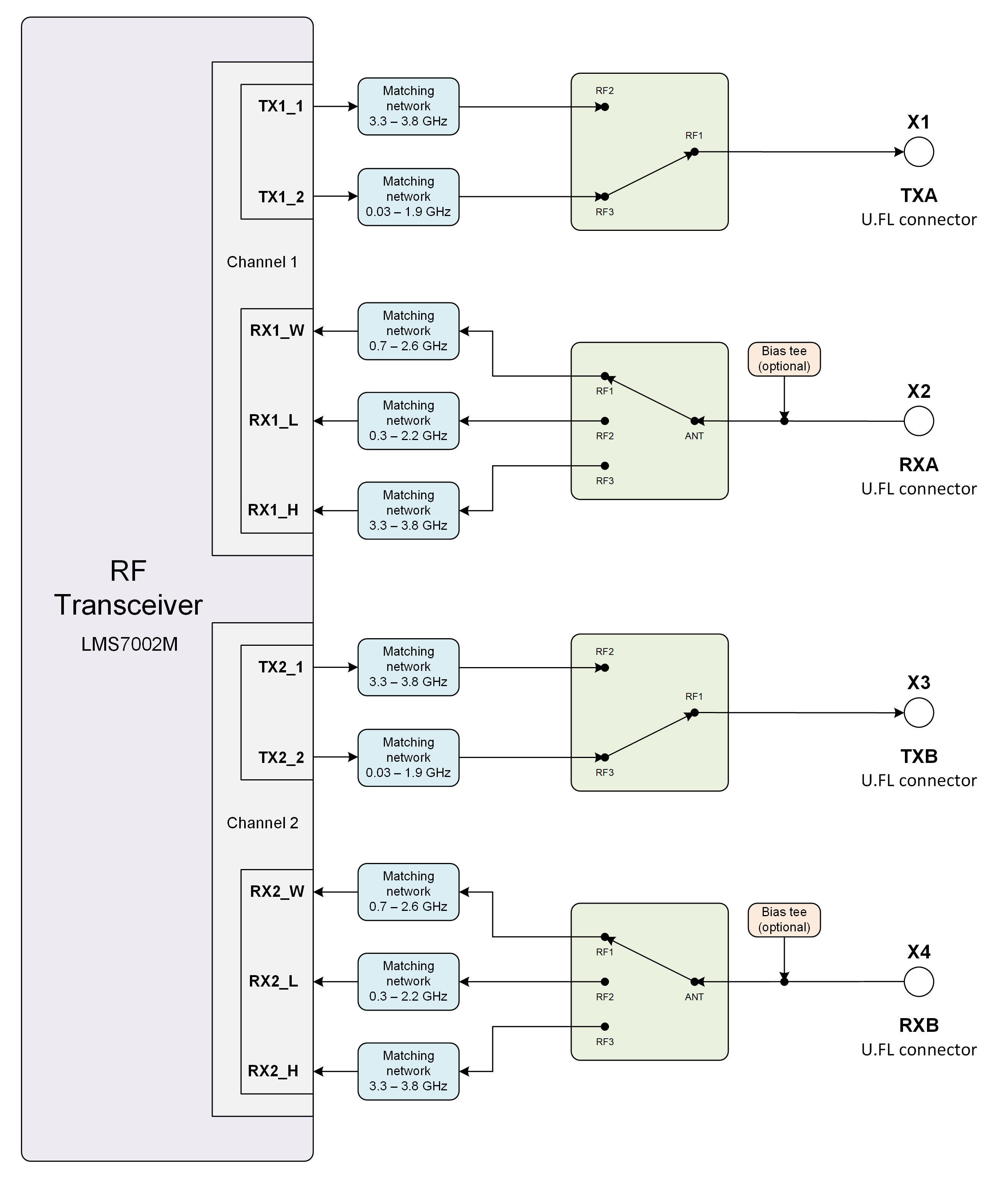
Figure 1. LimeSDR XTRX v1.2 RF diagram
LMS7002M RF transceiver TX and RX ports has dedicated matching network which determines the working frequency range. More detailed information on LMS7002M RF transceiver ports and matching network frequency ranges is listed in the Table 2.
LMS7002M RF transceiver port |
Frequency range |
|---|---|
TX1_1, TX2_1 |
2 GHz - 2.6 GHz |
TX1_2, TX2_2 |
30 MHz - 1.9 GHz |
RX1_H, RX2_H |
2 GHz - 2.6 GHz |
RX1_W, RX2_W |
700 MHz - 900 MHz |
RX1_L, RX2_L |
300 MHz – 2.2 GHz |
RF network switches are controlled via 2.4V logic signals. This is achieved by resistor dividers connected between FPGA (TX_SW, RX_SW1, RX_SW2) and switch control pin (TX_SW_DIV, RX_SW1_DIV, RX_SW2_DIV). RF network control signals are described in the Table 3.
Component |
Schematic signal name |
I/O standard |
FPGA pin |
Description |
|---|---|---|---|---|
SKY13330-397LF(IC5 and IC6) |
TX_SW/TX_SW_DIV |
3.3V |
P1 |
FPGA 3.3V logic level signal divided to 2.4V logic level. |
SKY13414-485LF(IC3 and IC4) |
RX_SW1/RX_SW1_DIV |
3.3V |
K3 |
FPGA 3.3V logic level signal divided to 2.4V logic level. |
RX_SW2/RX_SW2_DIV |
3.3V |
J3 |
FPGA 3.3V logic level signal divided to 2.4V logic level. |
LMS7002M baseband connectors
LMS7002M RF transceiver (IC1)) baseband signals (RX ADC and TX DAC) can be accessed via 0.3mm pitch 15 pin FPC connectors (X13 and X8). RX DAC connector pinout is shown in Table 4. TX ADC connector pinout is shown in Table 5.
Pin |
Schematic signal name |
Description |
|---|---|---|
1 |
GND |
Ground |
2 |
DAC1Q_P |
Channel 1 quadrature signal differential positive |
3 |
DAC1Q_N |
Channel 1 quadrature signal differential negative |
4 |
GND |
Ground |
5 |
DAC1I_P |
Channel 1 in-phase signal differential positive |
6 |
DAC1I_N |
Channel 1 in-phase signal differential negative |
7 |
GND |
Ground |
8 |
GPIO13 |
General purpose input/output (FPGA pin T17) |
9 |
GND |
Ground |
10 |
DAC2Q_P |
Channel 2 quadrature signal differential positive |
11 |
DAC2Q_N |
Channel 2 quadrature signal differential negative |
12 |
GND |
Ground |
13 |
DAC2I_P |
Channel 2 in-phase signal differential positive |
14 |
DAC2I_N |
Channel 2 in-phase signal differential negative |
15 |
GND |
Ground |
Pin |
Schematic signal name |
Description |
|---|---|---|
1 |
GND |
Ground |
2 |
ADC1I_P |
Channel 1 in-phase signal differential positive |
3 |
ADC1I_N |
Channel 1 in-phase signal differential negative |
4 |
GND |
Ground |
5 |
DAC1Q_P |
Channel 1 quadrature signal differential positive |
6 |
DAC1Q_N |
Channel 1 quadrature signal differential negative |
7 |
GND |
Ground |
8 |
GPIO13 |
General purpose input/output (FPGA pin T17) |
9 |
GND |
Ground |
10 |
ADC2I_P |
Channel 2 in-phase signal differential positive |
11 |
ADC2I_N |
Channel 2 in-phase signal differential negative |
12 |
GND |
Ground |
13 |
ADC2Q_P |
Channel 2 quadrature signal differential positive |
14 |
ADC2Q_N |
Channel 2 quadrature signal differential negative |
15 |
GND |
Ground |
USB 2.0 controller
LimeSDR XTRX could be powered and programmed via USB 2.0 by connecting it to micro-B port or mini PCIe connector. USB 2.0 is implemented using Microchip USB3333E-GL transceiver [link]. The controller signals description are shown below:
USB_D[7:0] – 8-bit data interface is connected to FPGA.
USB_NRST, USB_NXT, USB_DIR, USB_STP – interface control signals.
USB_CLK – interface clock. Clock from transceiver is fed to XILINX FPGA.
USB_26M – interface clock. Clock from FPGA is fed to Lime transceiver.
USB 2.0 controller pins, schematic signal names, FPGA interconnections and I/O standard are described in Table 6.
Chip pin (IC19) |
Chip reference (IC19) |
Schematic signal name |
FPGA pin |
I/O standard |
|---|---|---|---|---|
C2 |
RESETB |
USB_NRST |
M18 |
3.3V |
E3 |
DAT7 |
USB_D7 |
C15 |
3.3V |
E4 |
DAT6 |
USB_D6 |
A14 |
3.3V |
E5 |
DAT5 |
USB_D5 |
A15 |
3.3V |
D4 |
DAT4 |
USB_D4 |
B15 |
3.3V |
D5 |
DAT3 |
USB_D3 |
A16 |
3.3V |
C4 |
DAT2 |
USB_D2 |
B16 |
3.3V |
C5 |
DAT1 |
USB_D1 |
A17 |
3.3V |
B4 |
DAT0 |
USB_D0 |
B17 |
3.3V |
A3 |
STP |
USB_STP |
C17 |
3.3V |
B5 |
NXT |
USB_NXT |
A18 |
3.3V |
A4 |
DIR |
USB_DIR |
B18 |
3.3V |
A5 |
CLKOUT |
USB_CLK |
C16 |
3.3V |
A2 |
REFCLK |
USB_26M |
E19 |
3.3V |
Indication LEDs
LimeSDR XTRX board comes with two green indicator LEDs. These LEDs are soldered on the top of the board near the USB Micro-B connector.
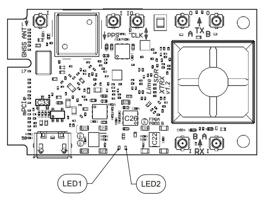
Figure 2. LimeSDR XTRX indication LEDs (top)
LEDs are connected to FPGA hence their function may be programmed according to the user requirements. Default LEDs configuration and description are shown in Table 7.
Board Reference |
Schematic name |
Board label |
FPGA pin |
Description |
|---|---|---|---|---|
LED1 |
FPGA_LED1 |
LED1 |
N18 |
User defined |
LED2 |
FPGA_LED2 |
LED2 |
V19 |
User defined |
Low speed interfaces
FPGA_SPI pins, schematic signal names, FPGA interconnections and I/O standards/levels are shown in Table 8.
Schematic signal name |
FPGA pin |
I/O standard |
Comment |
|---|---|---|---|
FPGA_SPI_SCLK |
W14 |
3.3V |
Serial Clock (FPGA output) |
FPGA_SPI_MOSI |
W16 |
3.3V |
Data (FPGA output) |
FPGA_SPI_MISO |
W15 |
3.3V |
Data (FPGA input) |
FPGA_SPI_LMS_SS |
W13 |
3.3V |
IC1 (LMS7002 (IC1)) SPI slave select (FPGA output) |
FPGA_CFG_SPI pins, schematic signal names, FPGA interconnections and I/O standards are shown in Table 9.
Schematic signal name |
FPGA pin |
I/O standard |
Comment |
|---|---|---|---|
FPGA_CFG_CCLK |
C11 |
3.3V |
Serial Clock (FPGA output) |
FPGA_CFG_CS |
K19 |
3.3V |
IC18 SPI slave select (FPGA output) |
FPGA_CFG_D00 |
D18 |
3.3V |
|
FPGA_CFG_D01 |
D19 |
3.3V |
|
FPGA_CFG_D02 |
G18 |
3.3V |
|
FPGA_CFG_D03 |
F18 |
3.3V |
FPGA_I2C1 (temperature sensor, EEPROM, CLK DAC, switching regulator) and FPGA_I2C2 (switching regulator) interface slave devices and related information are given in Table 10.
I2C slave device |
Slave device |
Inteface |
I2C address |
I/O standard |
Comment |
|---|---|---|---|---|---|
IC9 |
Temperature sensor |
FPGA_I2C1 |
1 0 0 1 0 1 1 RW |
3.3V |
TMP1075NDRLR |
IC13 |
EEPROM |
1 0 1 0 0 0 0 RW |
3.3V |
M24128 |
|
IC17 |
CLK DAC |
1 0 0 1 1 0 0 RW |
3.3V |
AD5693RACPZ |
|
IC22 |
Switching regulator |
1 1 0 0 0 0 0 RW |
3.3V |
LP8758A1E0YFFR |
|
IC31 |
Switching regulator |
FPGA_I2C2 |
1 1 0 0 0 0 0 RW |
3.3V |
LP8758A1E0YFFR |
To debug FPGA design, flash bitstream to FPGA and/or Flash memory JTAG X9 connector is used. It is located on the PCB bottom side (see Figure 5: LimeSDR XTRX v1.3 board bottom connectors and main components) and is compatible with Molex 788641001 connector. JTAG connector pins, schematic signal names, FPGA interconnections and I/O standards are listed in Table 11.
Connector pin |
Schematic signal name |
FPGA pin |
I/O standard |
Comment |
|---|---|---|---|---|
1 |
TDO |
W8 |
3.3V |
Test Data Out |
2 |
TDI |
W10 |
3.3V |
Test Data In |
3 |
TMS |
W9 |
3.3V |
Test Mode Select |
4 |
VCC3P3 |
Power (3.3V) |
||
5 |
TCK |
C8 |
3.3V |
Test Clock |
6 |
GND |
Ground |
GPIO connectors
Four GPIOs from FPGA are connected to 8 pin FPC connector (X12). GPIOS are separated by ground pins. Additional pin is dedicated for power as shown in Table 12.
Connector pin |
Schematic signal name |
FPGA pin |
I/O standard |
Comment |
|---|---|---|---|---|
1 |
VCC3P3 |
3.3V |
Power (3.3V) |
|
2 |
GPIO9_P |
H1 |
3.3V |
|
3 |
GND |
3.3V |
Ground |
|
4 |
GPIO9_N |
J1 |
3.3V |
|
5 |
GND |
3.3V |
Ground |
|
6 |
GPIO11_P |
K2 |
3.3V |
|
7 |
GND |
3.3V |
Ground |
|
8 |
GPIO11_N |
L2 |
3.3V |
Clock Distribution
LimeSDR XTRX board clock distribution block diagram is as shown in Figure 3.
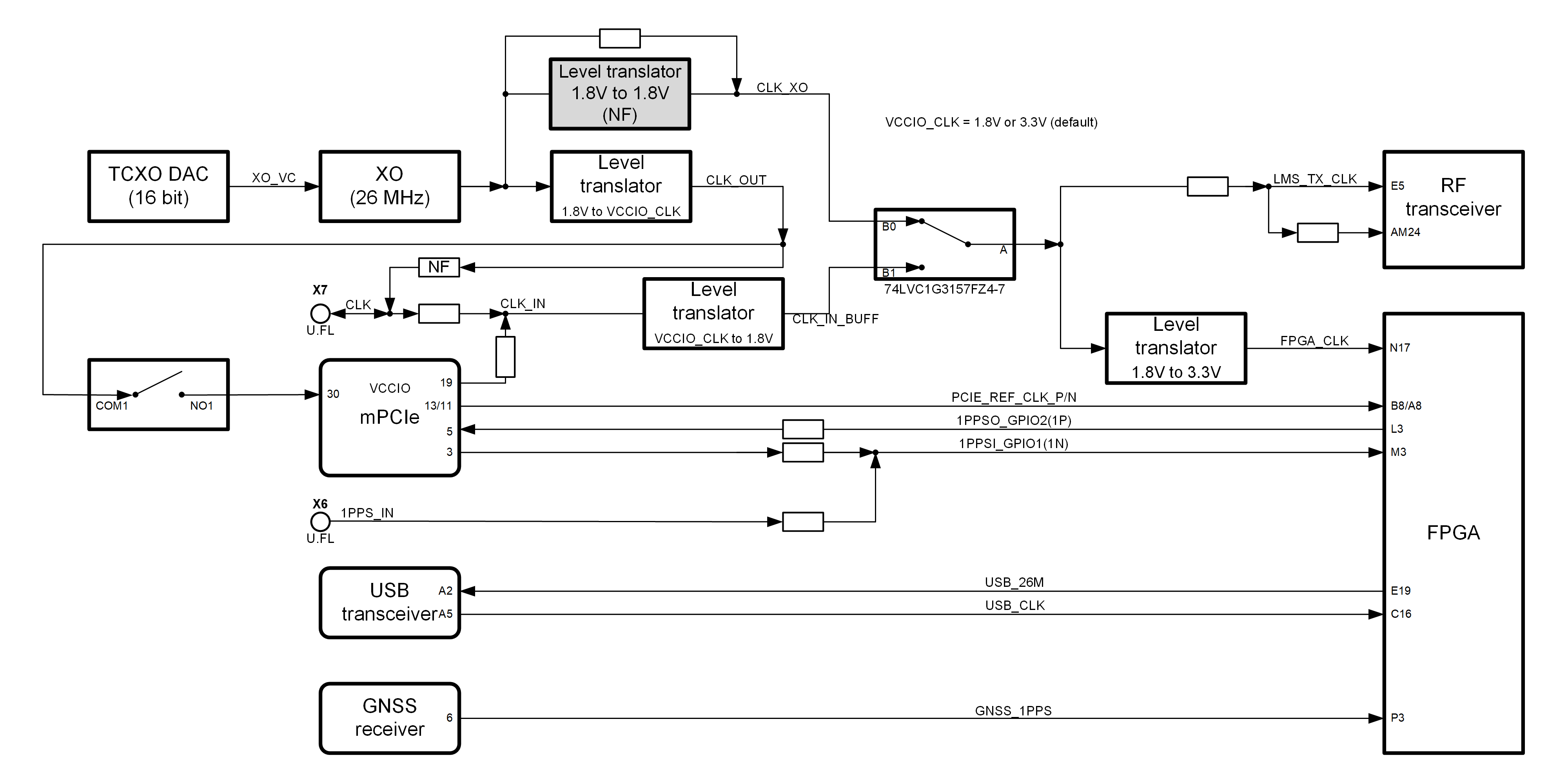
Figure 3. LimeSDR XTRX v1.2 board clock distribution block diagram
LimeSDR XTRX board features an on board 26.00 MHz VCTCXO as the reference clock for LMS7002M RF transceiver and FPGA PLLs.
Rakon E6982LF 26.00 MHz voltage controlled temperature compensated crystal oscillator (VCTCXO) is the clock source for the board. VCTCXO frequency may be tuned by using 16 bit DAC (IC17). Main VCTCXO parameters are listed in Table 13.
Frequency parameter |
Value |
|---|---|
Calibration (25°C ± 1°C) |
± 1 ppm max |
Stability (-40 to 85 °C) |
± 0.2 max |
Long term stability (1 year, 3 years) |
± 1 ppm max, ± 2 ppm max |
Control voltage range |
0.5V .. 2.8V |
Frequency tuning |
± 3 ppm |
Slope |
+4 ppm/V |
Analogue switch gives option to select clock source for RF transceiver and FPGA from buffered VCTCXO onboard clock XO1 (CLK_XO) and external U.FL (X7)/mPCIe (X10) sources (CLK_IN_BUFF). Buffered VCXO clock (CLK_OUT) can also be fed to other board using U.FL (X7)/mPCIe (X10)connectors.
The board clock lines and other related signals/information are listed in Table 14. VCCIO_CLK voltage can be selected between 1.8V and 3.3V (default).
Source |
Schematic signal name |
I/O standard |
FPGA pin |
Description |
|---|---|---|---|---|
External |
CLK_IN |
VCCIO_CLK |
External reference clock input |
|
Clock buffer (IC10) |
CLK_OUT |
VCCIO_CLK |
Reference clock output |
|
Clock buffer (IC14) |
FPGA_CLK |
3.3V |
A9 |
Reference clock connected to FPGA |
Analog mux (IC15) |
CLK_XO |
1.8V |
Reference clock connected to LMS |
|
RF transceiver (IC1) |
LMS_TX_CLK |
1.8V |
Reference clock input |
|
LMS_TX_CLK |
1.8V |
Reference clock input (0R) |
||
LMS_MCLK1 |
3.3V |
L17 |
||
LMS_FCLK1 |
3.3V |
G19 |
||
LMS_MCLK2 |
3.3V |
W5 |
||
LMS_FCLK2 |
3.3V |
W6 |
||
USB 2.0 controller (IC19) |
USB_CLK |
3.3V |
C16 |
Clock output from USB controller |
USB_26M |
3.3V |
E19 |
Clock input for USB controller |
|
GNSS Receiver (IC11) |
GNSS_1PPS |
3.3V |
P3 |
PPS output from GNSS receiver to FPGA |
FPGA (IC7) |
1PPSI_GPIO1(1N) |
3.3V |
M3 |
FPGA PPS input |
FPGA (IC7) |
1PPSO_GPIO2(1P) |
3.3V |
L3 |
PPS output from FPGA to X6 ND mPCIe pin 5 |
External |
1PPS_IN |
3.3V |
M3 |
PPS input for FPGA |
Power Distribution
As indicated, LimeSDR XTRX board may be powered via USB port (5V) or mini PCIe edge connector (3.3V). LimeSDR XTRX board power delivery network consists of different power rails/voltages, filters and power sequences. LimeSDR XTRX board power distribution block diagram is presented in Figure 4.
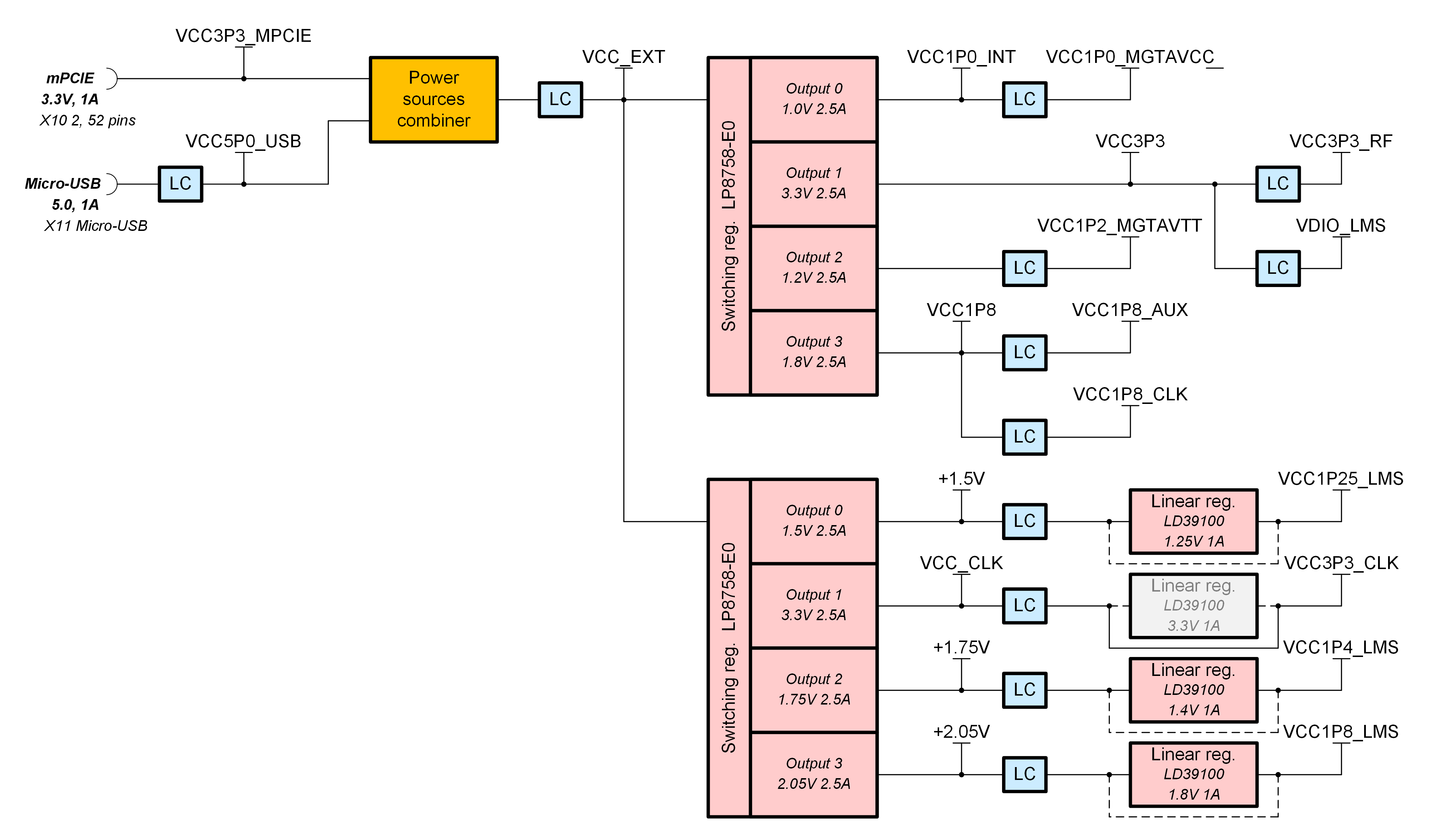
Figure 4. LimeSDR XTRX v1.2 board power distribution block diagram
Mini PCIe edge connector
LimeSDR XTRX board communicates with the host system via mPCIe connector. LimeSDR XTRX mini PCIe connector pinout and signals according to the specification is given in Table 15.
Pin |
Mini PCIe x1 Specification |
LimeSDR XTRX Schematic signal name |
Description |
|---|---|---|---|
1 |
Wake# |
NC |
Not connected |
2 |
3.3 Vaux |
VCC3P3_MPCIE |
Main power input 3.3V (VCC3P3_MPCIE) |
3 |
COEX1 |
1PPSI_GPIO1(1N) |
External 1PPS input or GPIO1 or GPIO1N, CMOS 3.3 V |
4 |
GND |
GND |
Ground |
5 |
COEX2 |
1PPSO_GPIO2(1P) |
GPS 1PPS output or GPIO2 or GPIO1P, CMOS 3.3 V |
6 |
GND |
NC |
Not connected |
7 |
CLKREQ# |
CLK_REQUEST# |
Tied to GND through resistor 330 Ohm |
8 |
UIM PWR |
UIM_VCC |
User Identity Module interface power 1.8 V or 3V |
9 |
GND |
GND |
Ground |
10 |
UIM_DATA |
UIM_DIO |
User Identity Module interface data 1.8 V or 3V |
11 |
REFCLK- |
PCI_REF_CLK_N |
PCI Express Reference clock differential pair negative signal |
12 |
UIM_CLK |
UIM_CLK |
User Identity Module interface clock 1.8 V or 3V |
13 |
REFCLK+ |
PCI_REF_CLK_P |
PCI Express Reference clock differential pair positive signal |
14 |
UIM_RESET |
UIM_RST |
User Identity Module interface reset 1.8 V or 3V |
15 |
GND |
GND |
Ground |
16 |
UIM_VPP |
NC |
Not connected |
17 |
Reserved |
TDD_GPIO3_N |
TDD TX Enable output or GPIO3N or GPIO4, CMOS 3.3V |
18 |
GND |
GND |
Ground |
19 |
Reserved |
CLK_IN |
External clock input 3.3 V |
20 |
W_DISABLE# |
TDD_GPIO3_P |
GPIO3P or GPIO3 (or Pair of TDD TX Enable), CMOS 3.3V |
21 |
GND |
GND |
Ground |
22 |
PERST# |
PCIE_PERST# |
PCI Express interface reset |
23 |
PERn0 |
PCI_TX0_N |
PCI Express interface output differential pair negative signal |
24 |
3.3Vaux |
NC |
Not connected |
25 |
PERp0 |
PCI_TX0_P |
PCI Express interface output differential pair positive signal |
26 |
GND |
GND |
Ground |
27 |
GND |
GND |
Ground |
28 |
1.5Volt |
NC |
Not connected |
29 |
GND |
GND |
Ground |
30 |
SMB CLK |
SMB_CLK |
Clock output (CLK_OUT) |
31 |
PETn0 |
PCI_RX0_N |
PCI Express interface input differential pair negative signal |
32 |
SMB Data |
SMB_DATA |
GPIO8 |
33 |
PETp0 |
PCI_RX0_P |
PCI Express interface input differential pair positive signal |
34 |
GND |
GND |
Ground |
35 |
GND |
GND |
Ground |
36 |
USB_D- |
USB_D_N |
USB 2.0 data differential pair negative signal |
37 |
GND |
GND |
Jumper to GND. Connected by default |
38 |
USB_D+ |
USB_D_P |
USB 2.0 data differential pair positive signal |
39 |
3.3Vaux |
PCI_TX1_N |
PCI Express interface output differential pair negative signal |
40 |
GND |
GND |
Ground |
41 |
3.3Vaux |
PCI_TX1_P |
PCI Express interface output differential pair positive signal |
42 |
LED_WWAN# |
LED_WWAN#_GPIO5 |
Output for LED WWAN (Negative) or GPIO5 3.3 V |
43 |
GND |
GND |
Jumper to GND. Connected by default |
44 |
LED_WLAN# |
LED_WLAN#_GPIO6 |
Jumper to GND. Connected by default |
45 |
Reserved |
PCIE_RESERVED |
Connected to FPGA (V7) |
46 |
LED_WPAN# |
LED_WPAN#_GPIO7 |
Output for LED WPAN (Negative) or GPIO7 3.3 V |
47 |
Reserved |
PCI_RX1_N |
PCI Express interface input differential pair negative signal |
48 |
1.5Volt |
NC |
Not connected |
49 |
Reserved |
PCI_RX1_P |
PCI Express interface input differential pair positive signal |
50 |
GND |
GND |
Ground |
51 |
Reserved |
PCIE_W_DISABLE2# |
Connected to FPGA (W3) |
52 |
3.3Vaux |
VCC3P3_MPCIE |
Main power input 3.3V (VCC3P3_MPCIE) |